Basics of Photovoltaic Device Operation
Most solar cells are based on slabs of semiconductor material (often silicon) with controlled doping (impurity addition) such that light is strongly absorbed into a diode structure – and the built-in electric field within the diode structure is strong enough to separate the photo-generated electron-hole pairs so that light is converted into electricity.
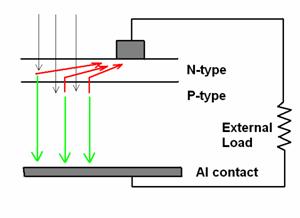
In this figure the light comes in from the top and is absorbed in the semiconducting material (either the n-type or the p-type part of the structure). After absorption the photo-generated electrons are swept toward the top contact (red arrows) and holes are conducted downwards (green arrows). The top contact is a thin finger electrode that draws current out from a narrow strip of the top of the cell. The top contact has to be narrow because light does not penetrate through metal and so any metal-covered-area represents some amount of lost efficiency.
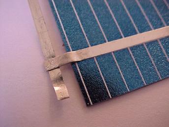 This
figure shows a solar cell where the silverish lines are the top metal
electrodes and the blue/black material is the silicon wafer (with an
antireflection coating on top, too).
This
figure shows a solar cell where the silverish lines are the top metal
electrodes and the blue/black material is the silicon wafer (with an
antireflection coating on top, too).
Within the semiconducting material where the light is absorbed, the nature of the p-type and n-type material junction is very critical in determining the output performance of the solar cells that we fabricate. These features are important:
- The band gap (Eg) of the primary absorbing material à this determines which photons of light will be absorbed effectively and which will not. Those photons with energy lower than Eg will not be absorbed by the structure. But the band gap also gives a measure of how high the output voltage could be (if optimized). Bigger Eg means higher voltage but lower current (because fewer photons absorbed). The best band-gap value is determined in relation to the solar spectrum that is available à as described initially in Shockley and Queisser’s seminal paper examining this trade-off (“Detailed Balance Limit of Efficiency of PN Junction Solar Cells”, J. Appl. Phys. 32 (1961) 510-519).
- The impurity concentration in the p-type and n-type regions (different elements, and could be different concentrations, too). These doping concentrations are important for two competing effects and properties. Higher concentration of these impurities usually leads to a larger voltage output from the cell. However higher concentrations also lead to thinner depletion layers at the contacting zone where the n-type and p-type are in contact with each other. This leads to a thinner “active” region where light can be absorbed by the material and tends to lower efficiency. Clever solar cell designs can partly get around this problem by building p-i-n diode structures where a thickness of intrinsic material is interposed between the n-type and p-type layers.
- The crystal quality of the material. The photogenerated current must not be permitted to recombine or experience resistive losses during the conduction through the cell structure. Recombination can happen at crystal defects, including dislocations, impurities, and surfaces. Resistive loss can come from intrinsic material mobility values or from non-linear contact resistance effects.
For further information about
solar cell operation, design, and fabrication, you might be interested in
signing up for the class that I teach on this topic. Visit this link to find
out more about “MSE 405 - Solar Cell
Design and Processing”
© Copyright, 2006, Dunbar P. Birnie, III,